Introduction
This module was written in response to repeated request for one-shot data acquisition with Xillybus at bandwidths that are above what Xillybus makes possible (or even the PCIe interface itself). As the FPGA boards involved often have DDR RAM memories with a much larger bandwidth capability, it’s appealing to suggest using the DDR memories as the immediate target for the data, and then move the data further to the computer with Xillybus at a slower pace. However that requires some kind of logic to get the data on and off the DDR memories.
With the module suggested on this page, it’s roughly a matter of replacing the existing FIFO between Xillybus and the application logic with another FIFO, having a depth measured in Gigabytes.
But it’s a wider issue: In many FPGA applications there’s a need for a plain, standard FIFO that is substantially deeper than possible with the memory resources given by the FPGA itself. The obvious solution is to utilize external memory, in particular when working on a development board which has DDR memories on board anyhow.
Surprisingly enough, there’s currently no immediately available solution for this. While Xilinx supplies a Virtual FIFO Controller in Vivado’s IP catalog, it’s hardly an extension of a standard FIFO, but rather a storage controller for bursts of data.
This page presents a Verilog module, deepfifo, that implements a virtual FIFO with a standard FIFO API. Based upon some external storage, which is supplied to deepfifo in the form of an AXI slave, deepfifo mimics the behavior of a standard FIFO with the depth allowed by this external storage.
Regarding the AXI slave, Xilinx’ MiG IP is the natural candidate for DDR memories. For Zynq devices, one of the processor’s AXI slave port can be used to allow the deepfifo module to use the processor’s memory space as a RAM storage (making sure that the software doesn’t write to the relevant memory segment, of course).
Except for the AXI slave, deepfifo also requires two standard (and fairly shallow) dual-clock FIFOs for immediate buffering and clock domain crossing.
Important: The deepfifo module is given at no cost, is not a product supplied by Xillybus, and is offered without support. Even though it has been tested rather rigorously on a KC705 board’s DDR memories, end users are solely responsible for its deployment in their projects.
For comments and questions, the “Other topics” section of this site’s forum is suggested.
Designing with deepfifo
This page focuses on using the deepfifo module. The design of deepfifo itself is explained on this page.
- Click here to download the deepfifo Verilog module
- Click here to download an instantiation example
This is a block diagram of the virtual FIFO:
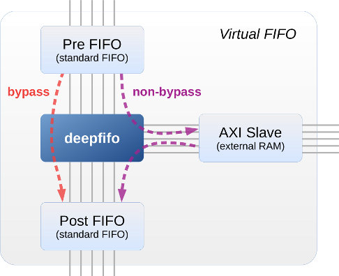
The virtual FIFO consists of four instantiated modules:
- The deepfifo module
- A memory controller or other AXI slave with memory functionality
- Two standard FPGA dual-clock FIFOs, with read and write count outputs: The Pre FIFO and Post FIFO.
None of the deepfifo module’s ports are exposed to the virtual FIFO’s ports. Rather, the virtual FIFO’s ports consist of one FIFO interface for writing words, one for reading words, and the ports required by the AXI slave to implement its functionality (e.g. direct I/O ports to a DDR memory).
As suggested by the block diagram, data from the Pre FIFO is bypassed to the Post FIFO as long as they are deep enough to contain the required number of elements (”bypass mode”). As soon as this storage depth isn’t enough, a buffer in the external RAM is used to create the illusion of a FIFO with the capacity of this buffer (”non-bypass mode”). The transition from bypass mode to non-bypass mode (and back) is automatic and transparent to the user of the virtual FIFO, of course.
From the point of view of the application logic that uses the virtual FIFO, it behaves exactly like a standard FIFO, only a lot deeper than usual: There is no particular restriction on how the data is organized. Under the hood, deepfifo uses fixed-size bursts on the AXI slave to ensure efficient use of the RAM resource, and avoid alignment issues. This is however transparent to the application logic: Thanks to the bypass mechanism, even a single word in the virtual FIFO is always visible on the read port within a few clocks.
The difficult part of using deepfifo is setting up the memory controller. If it’s a Xilinx MiG controller, follow the instruction for configuring an AXI-based controller for your board. Be sure that it has calibrated properly before attempting to use it with deepfifo (typically by monitoring its init_calib_complete port).
If a Zynq processor’s memory is used for storage, care must be taken to keep the processor away from the memory segment allocated for deepfifo’s buffer.
Note that the deepfifo module, the AXI slave and one half of each of the two FIFOs are clocked by the AXI bus clock, which is most likely supplied as an output from the AXI slave (or some component related to it).
A possible inconvenience with DDR controllers is that the memory controller’s data word width is very wide (512 bits is common for SODIMMs, for example). This can be solved by using asymmetric FIFOs for reformatting the application data into the controller’s word width. In this case the Pre and Post FIFOs won’t be identical, but will have opposite data port widths. Still, they must be equal in their depth on the side facing deepfifo.
Alternatively, an AXI Interconnect IP module with different data word widths can be inserted between deepfifo and the AXI slave. This is the preferred solution if several virtual FIFOs share the same memory resource (i.e. the same AXI slave).
deepfifo’s instantiation parameters
- addr_width: The width of the AXI address port (default is 32).
- base_addr: The lowest AXI address of the buffer for use by deepfifo (the base address of the RAM buffer)
- log2_ram_size_addr: The base-2 logarithm of the size of the RAM buffer, in bytes, that is log2(highest AXI address + 1 - lowest AXI address).
- log2_word_width: The base 2 logarithm of the word width of the AXI data interface (as well as the FIFO data width).
- log2_fifo_words: The base 2 logarithm of the depth (number of words) each of Pre and Post FIFOs has. If the FIFO is asymmetric, this relates to the words as seen on the side facing the deepfifo module. For example if each of these FIFOs has 512 words, the value of this parameter is 9.
- log2_burst_words: The base 2 logarithm of the AXI burst size, counting data words (not bytes). Note that a value above 4 (i.e. 16 word bursts) requires an AXI4-compatible slave (as opposed to AXI3). A value of 0 is legal (single-word bursts), but may cause a trivial synthesis error.
- fifo_threshold: The minimal number of words in the Pre FIFO for switching to non-bypass mode, i.e. that causes the use of the RAM buffer for storing data (as opposed to bypassing them directly to the Post FIFO).
The FIFOs must be at least twice as deep as the size of the AXI burst size (log2_fifo_words >= log2_burst_words + 1), but a minimum of four times deeper is recommended. For most purposes, FIFOs consuming one FPGA block RAM each are large enough.
Note that fifo_threshold is not given as a logarithm of the value, and doesn’t need to be a radix-2 number. In the absence of any particular considerations, setting it to half the FIFO’s depth is reasonable.
Bandwidth considerations
deepfifo is designed to efficiently utilize the bandwidth supplied by the AXI slave by queuing bursts in advance for the sake of maintaining a continuous data flow when possible.
Experimenting with KC705, an average writing rate of 11022 MB/s was attained with the on-board SODIMM, implemented with the example design’s parameters (800 MHz DDR clock = 1600 MT/s). This is ~92% of the theoretical limit of 8 x 1600 = 12800 MB/s. The exact same bandwidth result was reached regardless of whether the burst size was 16 or 256 words.
This result was attained on a write only session (the virtual FIFO wasn’t drained while data was pushed into it). When the virtual FIFO is filled and emptied at the same time, the AXI slave decides how to divide its capabilities between read and write requests. The arbitration policy can be selected in MiG’s IP configuration interface, and should be adjusted for the application’s needs.
It may be beneficial to set the burst length to the data amount equivalent to the underlying DDR memory’s row. This may reduce the impact of the row select to data access delay, which is inherent to any dynamic RAM, by (hopefully) preventing row deselection and re-selection due to interleaving between reads and writes.
Connecting AXI signals
The deepfifo module has several ports with the “axi_” prefix, which should be connected to the corresponding ports on the AXI slave (e.g. deepfifo’s axi_wready goes to a MiG controller’s s_axi_awready).
Several AXI ports of the AXI slave are not connected to the deepfifo module, as they are unrelated to its functionality.
The following AXI slave outputs (if present) should be left unconnected: axi_bid, axi_bresp, axi_rid and axi_rresp.
The following AXI slave inputs (if present) should be set to zero: axi_awid, axi_awlock, axi_awprot, axi_awqos, axi_arid, axi_arlock, axi_arprot and axi_arqos.
axi_awcache and axi_arcache (if present) relate to caching by the AXI slave, and are most likely ignored by MiG, and should be set to zero as well. In the case of a processor’s AXI slave, refer to its documentation for an adequate setting.
As for other AXI ports, refer to the slave’s documentation.
Other deepfifo ports
- clk (input): The module’s clock, which is the AXI clock and the clock to the FIFOs on the side facing deepfifo. When interfacing with a MiG controller, connect to its ui_clk port.
- reset (input): Asynchronous reset, active high. Should reset the pre and post FIFOs as well. Brings the virtual FIFO to an empty state and bypass mode.
- axi_aresetn (output): A reset signal synchronized to the AXI clock, exposed for convenience. Connect to AXI slave’s axi_aresetn port if it’s an input, or leave unconnected otherwise. Connect to a MiG controller’s aresetn input.
- fifo_pre_rd_en, fifo_pre_dout, fifo_pre_empty, fifo_pre_rd_count: Connect to the respective ports of the Pre FIFO (fifo_pre_rd_count to the FIFO’s read fill counter, rd_data_count).
- fifo_post_wr_en, fifo_post_din, fifo_post_full, fifo_post_wr_count: Connect to the respective ports of the Post FIFO (fifo_post_wr_count to the FIFO’s write fill counter, wr_data_count).
Improving timing closure
Even though there have been no issues with meeting timing with deepfifo on KC705, it’s worth pointing out a path that may be problematic and is relatively easy to fix: The deepfifo module contains combinatoric dependencies between the AXI slave and the FIFOs:
- fifo_pre_rd_en depends combinatorically on axi_wready
- fifo_post_wr_en depends combinatorically on axi_rvalid
If these paths cause timing difficulties, two measures are recommended:
For the Post FIFO: add a single clock delay on fifo_post_wr_en and fifo_post_din (i.e. sample these with a register), and connect the Post FIFO’s almost_full signal to fifo_post_full, so it considers the FIFO full at least one entry earlier.
For the Pre FIFO, wrap the original FIFO with reg_fifo as suggested on this page. The Verilog code can be copied as is, except that the FIFO’s rd_data_count needs to be exposed to reg_fifo’s ports.
Both of these two measures add a layer of registers, causing the values of the FIFOs’ rd_data_count and wr_data_count ports not to accurately represent the actual number of elements in the respective FIFOs anymore. This is not a problem, as deepfifo is designed to tolerate an inaccuracy of up to 8 elements of both these counters. Hence there is no need to add logic for adjustment of these values — they are good enough for deepfifo’s purposes despite this inaccuracy.