Introduction
Implementing a PCIe interface on Xilinx' Versal ACAP devices can prove trickier than with previous FPGA families, mainly because the structure of Xilinx' IPs has changed significantly. This is an attempt to shed some light on this topic.
Note that an easy-to-follow example design for Versal can be downloaded at Xillybus' PCIe download page. Please follow the Getting Started guides in the documentation page for a rapid setup.
The PCIe block on Versal FPGAs is in essence the same as the one in Ultrascale+ devices, however the procedure for setting up this interface is completely different. There are in fact two different ways for doing this:
- Creating an instance of a Versal ACAP Integrated Block for PCI Express IP.
- Utilizing the Control, Interfaces & Processing System (CIPS) IP.
Xillybus' example design is based upon the first option. This choice was made because the computer failed to boot with the CIPS-based PCIe implementation, despite extensive attempts to solve this problem.
However, regardless of how the PCIe block is implemented, a CIPS block must exist in the system. Hence there's no escape from having a basic understanding on this block.
Either way, the API with the application logic that uses the PCIe interface is exactly the same as Ultrascale+, as far as the AXI streams are concerned. This is also the case with those additional ports that are directly related to the core functionality of the IP. In particular, the API for delivering interrupts, keeping track of credits etc. is the same, except for slight and obvious changes in the names of the ports.
In the vast majority of use cases, the migration of a design for Ultrascale+ to Versal is just a matter of configuring the IP block in an equivalent manner and rewriting its instantiation. This holds true for both options above.
That said, there are some minor differences on the ports that have to do with the PCIe block's finer details. Those differences are listed in the product guides (see Appendixes of pg343 or pg346, as applicable).
Before discussing the PCIe options, there's no way around understanding some basic concepts regarding the Versal devices. Remember that there's no way avoiding this anyhow. Get ready for some PMC, CPM, CIPS.
PMC, PS and PL
As there's no choice but to configure the CIPS sooner or later, it's important to know about the PCM, PS and PL trio in a Versal device:
- The PMC (Platform Management Controller). A small processing system, consisting of a Microblaze-architecture processor. This processor brings up the entire device on powerup by running the initial bootstrap code, some of which is part of the "Device image" that is created by Vivado upon the implementation of an FPGA project. After the bringup, this processor continues to maintain simple housekeeping tasks. For the purpose of implementing PCIe, the importance of this block is related to the PCIe's reset (PERST) input, as explained further below.
Quite obviously, this Microblaze processor is implemented directly on silicon, and not in logic fabric. After all, it has to be there at the very beginning. - The PS (Processing system): An ARM Cortex-A72 processor, suitable for running a fullblown Linux system, or bare-metal application code. There's no need to run anything on this processor, and it can be ignored. But it's important not to confuse it with the PMC in the documentation and when setting up the CIPS.
- The PL (Programmable Logic, what most of us call the "FPGA"): The logic fabric and the dedicated logic tiles (block RAMs, multipliers, clock resources, GTY transceivers, the PCIe blocks etc.).
Note that Versal devices are configured differently from traditional FPGAs. The standalone bitstream (.bit file) is gone, and instead the Versal family has a programmable device image (PDI) that includes, among a lot of other things, the configuration frame data for the PL part. So for the purpose of a simple FPGA project, the PMC is loaded first, and then it loads the "FPGA part" (PL).
The CPM
For the purpose of implementing a PCIe interface, the CPM unit and the PCIe block are the same thing. Or more precisely, the CPM is a sub-block inside the CIPS IP, which can be configured to expose the ports of the PCIe blocks to application logic. For example, a VCVM1820 FPGA has two PCIe blocks, so the CPM can expose both.
Unlike the traditional PCIe blocks, the CPM can be configured to expose the PCIe blocks in various interface standards. This includes the same AXI-ST interface as Ultrascale+, but also as an AXI bridge for memory/address to the PCIe bus, as well as other interfaces, e.g. NoC (Network on Chip) and CCIX (Cache Coherent Interconnect for accelerators). So the CPM is a collective name for anything that can be done with the PCIe blocks of the FPGA. Instead of several IPs that expose a different interface each, there's the CPM, which is included in the CIPS IP.
There's no official explanation to what the acronym CPM stands for. Xilinx' AM016 says it's an "Integrated block for PCIe with DMA and cache coherent interconnect" (in its "Acronyms" section).
A brief introduction to the CIPS
The CIPS IP (Control, Interfaces and Processing System) is a block that contains two completely different units: One PS/PMC unit (which is a PS9 processing system, containing both processors), and one CPM unit.
This sounds more complicated than it actually is, in particular for those who are not interested in those extra functionalities.
The first question that comes to mind is why these two units are mixed into a single IP block. So it's worth to keep in mind that Versal was designed for high-performance computing tasks in datacenters. When used for other applications, this IP's structure seems quite unnatural.
So it's just a matter of getting used to that this IP has two purposes: The first purpose is to contain the information on how the device should be configured (in particular the PMC and PS). That allows Vivado to set up the part in the PDI that (more or less) tells the PMC which PMC/PS register should get what value. The second purpose is to optionally expose the PCIe blocks.
So when a CIPS is first put in the block design, it looks like this:
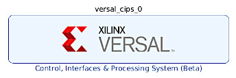
This is a block with no I/Os, because none of the PCIe blocks has been enabled in the CPM unit. But it's not redundant: Trying to implement a design without a CIPS somewhere in the FPGA design results in the DRC failing at the Write Device Image stage with
[DRC CIPS-2] Versal CIPS exists check - wdi: Versal designs must contain a CIPS IP in the netlist hierarchy to function properly. Please create an instance of the CIPS IP and configure it. Without a CIPS IP in the design, Vivado will not generate a CDO for the PMC, an elf for the PLM.
On the other hand, this is what the CIPS block looks like after enabling PCIe controller 0 in "PCIe mode":
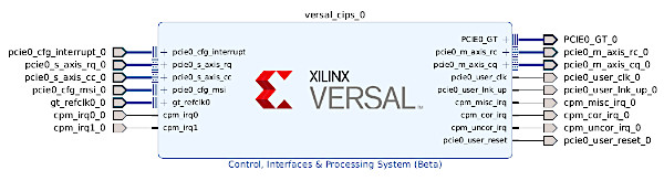
By connecting the CIPS block's interfaces as the block design's external ports, the obtained block design can be instantiated and used just like any regular Ultrascale+ PCIe block. It's indeed somewhat confusing that there's a CIPS block inside, which is responsible for completely different tasks, but otherwise there's no problem with this.
As for the natural reluctance to configure a whole subsystem that has nothing to do with the desired application, the CIPS isn't a big deal: Its defaults are good enough to bring up the FPGA, so there's not much hassle with it.
The PCIe blocks that are not configured for use by the CPM (i.e. the exposed by the CIPS) can be utilized the old-school way, i.e. with the Versal ACAP Integrated Block for PCI Express IP. But there are good reasons to avoid this, as detailed below.
The PCIe bus' reset (PERST)
For reliable operation, any PCIe block must be connected to the PCIe bus' reset signal (PERST), so that the host can begin the peripheral's enumeration from clean. On top of the obvious need to reset the block properly.
There are two alternatives to connecting this reset signal to a Versal FPGA:
- To an MIO pin, i.e. a pin that is available only to the PS or PMC processors.
- To a general-purpose PL ("FPGA") pin, which is available only to the PL part.
Given that the PCIe blocks are part of the PL, it may seem obvious to choose the second option, but once again, it's the less preferred way to go. For example, in Xilinx' official development board, the PCIE_PERST_B net is connected to pin D19 on the VMK180 / VCK190, which is an MIO pin (MIO38 on PMC). In other words, it belongs to the Microblaze processor, and is not available directly to the PL ("FPGA") part.
By contrast, another development board, HTG-VSL1, has the same reset signal connected both to the PMC's MIO24 and a PL I/O pin.
Connecting the PERST to an MIO pin is a non-issue when the CIPS block is used as the PCIe block: Indeed, when the PCIe bus is reset, the signal reaches only the PMC physically, but the processor makes sure to reset the PCIe block as necessary. On the other hand, when the PCIe block is implemented with a PCI Express block outside of the CIPS, this reset signal has to be exposed by the latter.
In either case, if the PERST is connected to an MIO pin, the reset signal for the actual PCIe block is the one that goes through the Microblaze processor.
It may seem odd to connect the PERST to a processor rather than to the PL directly, however in a datacenter application, where the PCIe bus is the primary means to control the FPGA, the bus' reset may very well have a broader significance, which is probably why it makes sense to connect it to the system's main controller.
Note that if the PERST is connected only to a PL I/O pin, there is no documented way to use the CPM (i.e. the PCIe block inside the CIPS). By contrast, when the reset is connected to the dedicated MIO pin, both options are possible, which is why this is the preferred option.
To CPM or not to CPM
This discussion is possibly detached from reality, judging from the problems that were encountered while attempting to implement Xillybus' PCIe example design with a CPM: The computer wouldn't boot with a PCIe block of this sort.
There are nevertheless several disadvantages with choosing the Integrated Block for PCI Express IP:
- Unlike earlier FPGA families, the "Versal ACAP Integrated Block for PCI Express IP" doesn't include the transceivers and their infrastructure elements. The intended workflow is hence to create a block design that consists of the required components: The PCIe IP block itself plus other blocks for the transceivers and other elements. Even though these additional elements can be inserted into the block design by virtue of block automation, the result is significantly more difficult to maintain. In particular, changing the PCIe interface's speed and lane count requires regeneration of the surrounding blocks, as their attributes depend on the main PCIe block's raw link parameters.
- A CIPS IP must be present in all designs for Versal FPGAs anyhow, so there's no way around configuring this IP.
- The PCIe part in a CIPS is similar, and in fact better than the dedicated PCIe block. In particular, it's possible to opt out groups of ports that relate to unnecessary functionalities, so the instantiation in Verilog / VHDL is simpler and less error-prone.
- It's quite evident that Xilinx intended the CIPS to be the main player in a Versal FPGA.
There are however situations where the non-CIPS method is eligible:
- When the CIPS interface simply doesn't work (which is likely the case).
- When the PCIe block should not support low-power features (D1 and PME). Due to a bug, Vivado ignores the user's settings (as of 2022.1) and always sets the block to declare support of these. Alternatively, this can be worked around, as shown in this page.
- When the PERST (PCIe reset) pin is connected only to a regular FPGA I/O pin.
- When two PCIe blocks are instantiated in different places in the HDL's hierarchy.
- When the CPM's fixed pinout of PCIe lanes and reference clock is unsuitable.
- When there's a benefit for directly handling the transceivers.
- When an example design is necessary: The PCIe block for CPM doesn't have an example design (but Xillybus' demo bundle can be used as an example for how to set up the CIPS). See Appendix G of pg346, "Features Not Available".
How-to
The steps for getting the PCIe block configured, using the CPM inside the CIPS IP or not, are given in detail in Xilinx' own documentation. Finding exactly where it's documented might not be so easy, so these are some pointers:
Chapter 4 in the CPM Mode for PCI Express product guide (pg346) shows in detail how to configure the CIPS IP block to expose one PCIe block to application logic. Doing this involves configuring both the CPM and PCM parts of the CIPS. As for the CPM part, this means to enable the PCIe block, and then configure it with a set of menus that is very similar to those of the old-school PCIe blocks. After doing this, the PCM part is configured by selecting which MIO input is used as the reset input (it's most likely PMC MIO 24 or 38).
Those who want to implement the PCIe block with the dedicated Integrated Block for PCIe may use any general-purpose PL I/O pin for the PERST input. But if the reset is connected to an MIO pin, the CIPS must be configured to regarding the MIO input (the PCM part), exactly as described in pg346. The CPM configuration should be skipped in this case, or else would the CIPS take over the relevant PCIe block.
Appendix B of the Product Guide for Versal ACAP Integrated Block for PCIe (pg343) shows how to make the CIPS expose the PCIe reset signal to the PL in the section named "CPM4 Additional Considerations". In short, it consists of entering the PS/PMC configuration part in the CIPS' configuration GUI, select the Peripherals section to the left, and click on the "PCIe Reset" peripheral. And then check the "PL PCIE" checkbox. This is possible on Vivado 2021.2 and later.
Refer to Table 91 in the same pg343 for a list of allowed MIO locations.
Working with CPM
These are some additional notes on the CPM as a PCIe block. Once again, it's probably not a good idea to use CPM.
Turning the CIPS block into a PCIe block consists of the following steps:
- In the CPM subsystem, enable the PCIe controller 0 as PCIE, and select the desired lane width.
- Also in the CPM subsystem, set up the PCIe controller's attributes in the CPM4 PCIE Controller 0 Configuration/
- In the PCM/PS configuration, inside IO configuration, enable the CPM4 peripheral, and select the correct MIO pin for the bus reset.
The interface with the block is much neater than the old-school PCIe block, as it's possible to select which of the groups is required in the "Enable Interface Options". It's recommended to first enable them all, and then look at the graphic block's perimeter for the signals that are required. Because all interface options are off by default, it may appear as if the CPM's PCIe block has limited access, which isn't the case.
Note however that a lot of inputs that control various values in the configuration space has been removed, and can be set as "part of the register table" instead (see pg346, Table 69: Deprecated Ports).
There are two IRQ inputs (cpm_irq_0 and cpm_irq_1) which should be held low, according to pg347. There are also three IRQ outputs (cpm_cor_irq_0, cpm_misc_irq_0, and cpm_uncor_irq_0) which are reserved and should be ignored.
Building a PCIe block (the non-CIPS way)
First, add a Versal ACAP Integrated Block for PCI Express IP to an empty block design, and configure the PCIe block as desired. There should be no other block in that block design at this stage (i.e. delete everything else, including external ports, if such exist).
The click "Run block automation". Check "All automation" to the left (it most likely already is) and then select the link width and speed as desired. This must match the settings in the PCIe block.
Then select all pins of the PCIe block that aren't connected to anything (CTRL-click), and make them external with right-click > Make External. Ports are created for all, with a _0 suffix on the net's name.
There is an example design, so the constraints can be taken from there. There are a lot of constraints that are commented out in the example design's .xdc file, and they are apparently not necessary. The design builds properly and meets constraints without them.
Conclusion
Despite a whole lot of confusing issues and some new terminology, it's quite possible to migrate a design with a PCIe interface from Ultrascale+ to Versal devices. An important point with the latter devices is to pay attention to how the PERST pin is connected to the FPGA.
But with a few oddities out of the way, which may appear scary at first, a Versal device is quite similar to an Ultrascale+, at least regarding the PCIe block.